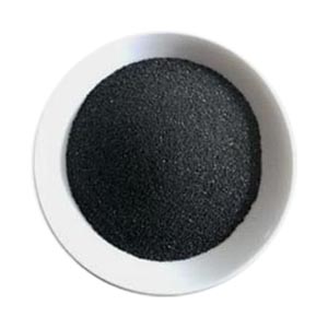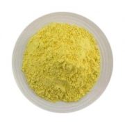

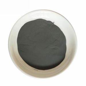
Bismuth selenide
Other name: Dibismuth triselenide, bismuth(iii) selenide, bismuth(3+) selenide (2:3)
CAS No. : 12068-69-8
Formula: Bi2Se3.
Molecular weight: 654.8408
Density (g/mL, 25 ℃) : 6.82
Melting point : 710℃
- 描述
- Inquiry
Appearance: Grey black powder or granule
Purity: 99.99%, 99.999%
Uses: for semiconductor materials and thermoelectric materials.
Nature: black crystal material. Rhombohedral hexagonal crystal structure. Insoluble in alkali, easily concentrated acid, aqua regia. By the direct reaction of selenium and bismuth or bismuth oxide and hydrogen selenide Preparation
Topological insulator is a new type of quantum material state discovered in recent years. It has great application prospect in energy-free transmission, spintronics and quantum computers. In addition to the singular topological surface states that are not scattered by defects and nonmagnetic impurities, the introduction of a spiral dislocation line defect into the topological insulator may also create a one-dimensional topological protected spiral state that creates a perfect conductive aisle. Graphene-like layered bismuth selenide Bi2Se3 is considered as one of the most promising topological insulator materials due to its simple band structure, much larger than the band gap of energy fluctuation at room temperature. China University of Science and Technology Hefei National Laboratory for Microscale Materials Science and Chemistry and Materials Science and Technology Professor Zeng Jie Group based on the characteristics of controlled preparation methods, starting from the kinetics of crystal growth theory, through the reaction system to maintain a very low Saturated conditions, the selenium bismuth in the nucleation process to produce spiral dislocation defects, thereby inducing the two-way spiral material layered growth, breaking the inherent selenium bismuth crystal growth mode. In addition, the researchers also through the spiral growth rate control, the synthesis of different levels of development of spiral structure, clarifying the two-dimensional layered material spiral growth mechanism. This study provides a material basis for achieving one-dimensional topological spiral states and helps to promote the new development of bismuth selenide in topological insulators, thermoelectric and catalytic. In addition, the way to explore helical growth is also an important guideline for the synthesis of the helical structure of other two-dimensional layered materials, thereby modulating the physical properties of the material
Scientists have prepared ultrathin bismuth selenide two-dimensional layered materials
Yu Xuefeng, Research Institute of Advanced Institute of Technology, Chinese Academy of Sciences, cooperated with Professor Wang Beiquan from Wuhan University and Professor Zhu Jianhao from City University of Hong Kong to prepare ultrathin bismuth selenide two-dimensional layered materials and apply it to photothermal imaging guided photothermal treatment. Relevant results have been reported as a cover article by Small Magazine.
In recent years, two-dimensional layered materials such as graphene have drawn more and more attention due to their unique properties and broad prospects. As a kind of two-dimensional layered materials, bismuth selenide has significant thermoelectric and optoelectronic properties, and has good biological activity and biocompatibility, aroused great interest of scientists. Particle size is crucial for functional optimization of two-dimensional layered materials, and two-dimensional materials of several atomic layer thicknesses tend to have good electrical and optical properties. At the same time, in biomedical applications, particle size not only affects cellular uptake and biocompatibility, but also affects its metabolism in the body. Therefore, how to prepare ultra-thin ultra-thin bismuth selenide nanosheets is a hot issue to be solved urgently in current applications.
In response to this problem, the research group has established a simple liquid-phase synthesis method to achieve the large-scale preparation of bismuth selenide. The resulting bismuth selenide nanosheets have a thickness of only 1.7 nm and a sheet size of about 31.4 nm. The study found that this ultra-thin bismuth selenide nanosheets have excellent near-infrared optical properties, the light-to-heat conversion efficiency of 34.6%. At the same time, it also has a high photoacoustic conversion efficiency, photoacoustic-guided photothermal therapy can be achieved, and can be effectively metabolized from the outside. The study confirmed that this ultra-thin bismuth selenide two-dimensional material has great potential in the field of biomedical photonics. (Source: China Science News)
相关产品
-
Cadmium telluride
Other name: Cadmium telluride Coating quality Balzers; telluroxocadmium
CAS no. : 1306-25-8
EINECS no. : 215-149-9
Molecular formula: CdTe.
Molecular weight: 240.011.
Density: 5.85 g / cm3
Melting point: 1092 ° C
Boiling point: 1130 ℃
-
Bismuth sulfate
Other name:
bismuth(3+) sulfate (2:3);bismuthtrisulfate;Bismuthous sulfate ; Dibismuth trisulfate, Bismuth trisulfate, Dibismuth tris(sulphate), dibismuth(3+) ion trisulfate
Cas number: 7787-68-0
Molecular formula: Bi2O12S3; Bi2 (SO4) 3
Molecular weight: 706.15
EINECS no. : 232-232-5
-
Bismuth trichloride BiCl3
Alias: Bismuth chloride, bismuth (+ 3) trihydride cation trichloride; Bismuth (Iii) Chloride;
Trichlorobismuth;trichloro-bismuthin
CAS no. : 7787-60-2
EINECS no. : 232-123-2
Formula: BiCl3
Molecular weight: 315.3394
-
Nanometer cobalt oxide
Other name: Cobaltosic Oxide,Tricobalt tetroxide, Cobalt Tetroxide
The CAS number: 1308-06-1
EINECS no. : 215-157-2
Molecular formula: Co3O4
Molecular weight: 240.7972
-
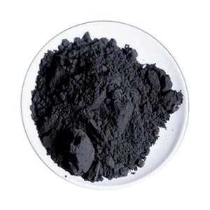
Bismuth telluride
Other name: Bismuth(III) telluride, dibismuth tritelluride; bismuth(3+) telluride (2:3)
Type N: doped Selenium
Type P: doped Antimony
Grain size: -60 mesh, -100 mesh, -200 mesh, 325 mesh
Electrical conductivity: 1050/950
Thermal conductivity: 1.35/1.3
Seebeck coefficient: 220/280
Test temp.: 300K -
Bismuth subcarbonate
Other name: Bismuth carbonate , Bismuth Subcarbonate, dibismuth carbonate dioxide
CAS No.: 5892-10-4
EINECS number: 227-567-9
Molecular formula: CBi2O5
Molecular weight: 509.9685 -
Nanometer Bismuth oxide
English alias: Bismuth tetroxide; Bismuth oxide (BiO2); Dibismuth oxygen anion (2);
CAS no. : 12048-50-9
EINECS no. : 234-985-5
Molecular formula: Bi2O3
Molecular weight: 465.959